🎩🎩🎩 𝗡𝗲𝘄 𝗟𝗮𝗯𝗲𝗹 𝗳𝗶𝗲𝗹𝗱𝘀 𝗶𝗻 𝗞𝗶𝗖𝗔𝗗 𝟳 The new KiCAD v7 brings a new opportunity for fields of a label. In the picture, you can see the new field „microstrip“, which is directly translated as a Net class identifier. 👉
Label fields
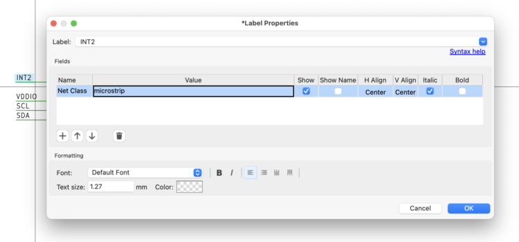

🎩🎩🎩 𝗡𝗲𝘄 𝗟𝗮𝗯𝗲𝗹 𝗳𝗶𝗲𝗹𝗱𝘀 𝗶𝗻 𝗞𝗶𝗖𝗔𝗗 𝟳 The new KiCAD v7 brings a new opportunity for fields of a label. In the picture, you can see the new field „microstrip“, which is directly translated as a Net class identifier. 👉
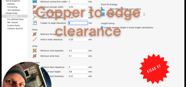
🎩🎩🎩 𝗞𝗶𝗖𝗔𝗗 𝘃𝟳 𝗮𝗻𝗱 𝗰𝗼𝗽𝗽𝗲𝗿 𝘁𝗼 𝗲𝗱𝗴𝗲 𝗰𝗹𝗲𝗮𝗿𝗮𝗻𝗰𝗲 What is this all about? The KiCAD v6 had the same design constraint as the new KiCAD v7. Both look the same but act differently. The new KiCAD v7 really pours the
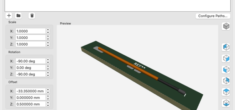
🎩🎩🎩 A 3-step guide on how to prepare a simple 3D model for KiCAD I have a very short guide on preparing a simple 3D model of a component for a KiCAD footprint. 1️⃣ Create a simplified body in FreeCAD.
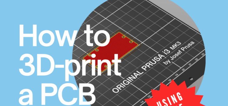
🎩🎩🎩 How to 3D-print PCBs from KiCAD? I prepared a short guide using Free tools only: 1️⃣ Set a new Drill/Place origin to the bottom left corner of the PCB. 2️⃣ Export the PCB as a new 3D model in
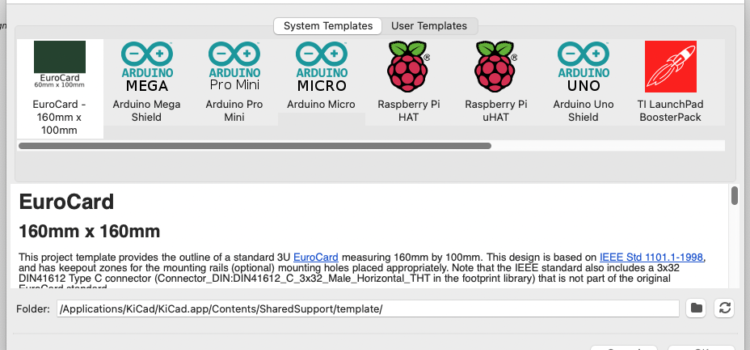
🎩🎩🎩 Project templates in KiCAD Work on #hardwaretemplates for @Beny-devices inspired me to simplify the schematic drawing preparation. Especially the drawing Title block content repeats in every project. Here is a short guide on how to prepare a customized KiCAD schematic template:
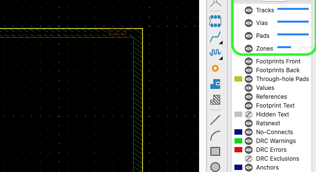
🎩🎩🎩 Object opacity in KiCAD Today, I have a small tip for KiCAD users who are not so observant. I am not, which is why I noticed the opacity sliders almost a year after the current version 6 leaked. You
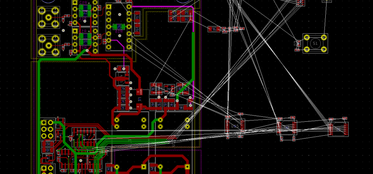
🎩🎩🎩 Repeat the last action in KiCAD is a killer feature 1️⃣ Place a label, a no-connection flag, you name it 2️⃣ Hit the Repeat the last action keyboard shortcut, CMD+I in my case 3️⃣ Hit as many times as
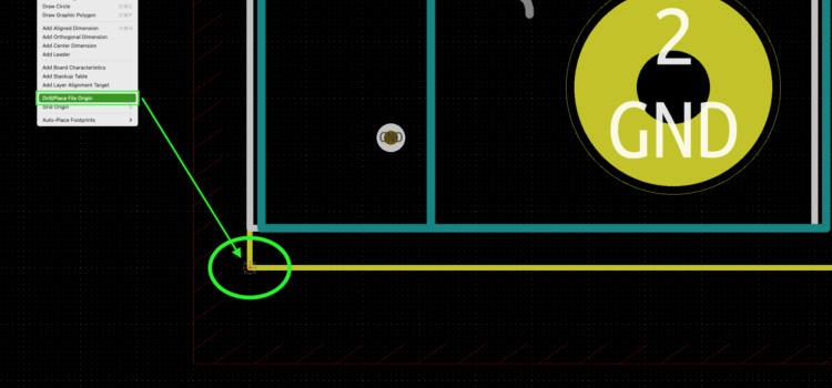
🎩🎩🎩 Drill/Place file origin in KiCAD There can be a discussion around this point. After a while, when learning how to use FreeCAD for KiCAD STEP model customisation, I found the Drill/Place file origin needed to be set. The default
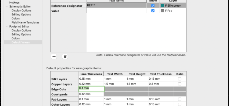
🎩🎩🎩 Edge cuts thickness in the KiCAD Footprint editor This tip deals with tiny detail settings for the Footprint editor. The default Edge cuts line thickness in the PCB editor is 0.10 mm. The default Edge cuts line thickness in
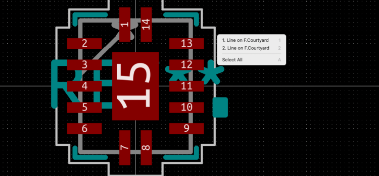
🎩🎩🎩 Footprinty stažené z Ultra Librarian Mám pro dnešek významný ale pravděpodobně hodně známý tip pro uživatele KiCADu, kteří využívají knihovní prvky z Ultra Librarian. ⚠️ Všechny Ultra Librarian footprinty, pravděpodně generované, obsahuji špatně definované hranice – courtyard. 1️⃣ Všechny